
The purpose of Design for Testing (DFT) in VLSI chips is to increase the accessibility of internal nodes.
Controllability: the ability to establish a specific signal value at each internal node by setting inputs.
Observability: ability to determine internal values by controlling inputs and observing outputs ensure predictable circuit responses.
Trade-offs
Technical: area, I/O pins.
Performance Economic: design time, yield, time to revenue.
DFT Design Rules
Adoption of DFT measures at the beginning stages of chip design leads to easier testing during manufacturing and debugging process.
The golden rules to be followed during Scan insertion are as follows
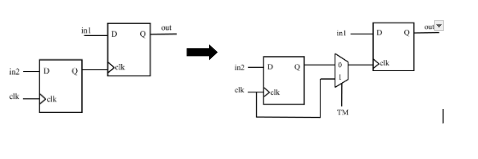
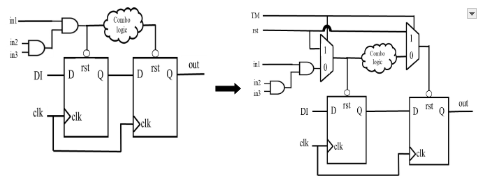
Derived clocks
Derived clocks are not directly controlled from the primary inputs. Hence to test the logic driven by these derived clocks, these clocks must be bypassed during entire test operation.
Ex: If clk=1 before the combinational logic, it should be visible after the combinational logic also. i.e. controllability.
Fixing derived clocks:
Here, TM=1, during test operation, so, the multiplexer selects primary clock CK signal, that is directly controllable.

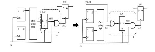
Gated Clocks
It is a good approach for reducing power consumption. But it prevents the clock ports of some flip-flops from being directly controlled by primary inputs.
Fixing gated clocks:
The clock enable signal (EN) is generated at the rising edge of CK and is loaded into the latch LAT at the failing edge of CK to become CEN. CEN is then used to enable or disable clocking for the flip-flop DFF. Modifications allow the scan shift operation to be conducted on these storage elements.

Clock as data input
Clock signal should not be used as data input in scan test mode. Here, the clock acts as one of the input to and gate, which makes the output of and gate less controllable, results in the loss of test coverage as use of clock as data input causes setup and hold violation.
Fixing clock as data issue:-


When TM=1, and gate output is not dependent on clk input, so timing issues with clk can be eliminated.


But, when TM=1, the output of or gate is always high irrespective of the other input. So, output will be stuck at 1. No possibility of output going 0, which reduces the test coverage. To improve the test coverage, mux can be used in place of or gate.


When TM=1, and gate output is not dependent on clk input.
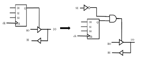
Bidirectional I/O ports
Bidirectional I/O ports are used to increase the data transfer bandwidth. During the shift operation, conflicts may occur at a bidirectional I/O port. During the capture operation, a bidirectional I/O port is usually specified as being either input or output.
Here, Bidirectional I/O port is used as an input and the direction control is provided by the scan cell. Because the output value of the scan cell can vary during the shift operation, the output tristate buffer may become active, which results in conflict if BO and the I/O port driven by the tester have opposite logic values.
Fixing tristate buffer issue:
Force the tristate buffer to make it inactive when SE = 1, and the tester is used to drive the I/O port during the shift operation.
During the capture operation, the applied test vector determines whether a bidirectional I/O port is used as input or output and controls the tester appropriately.

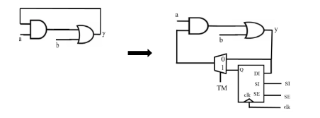
Combinational Feedback Loops
The value stored in the loop cannot be controlled or determined during test, this will increase the test generation complexity or loss in fault coverage. Hence, Combinational feedback loops are not a recommended design practice.
Fixing Combinational feedback loop issues
Rewrite the RTL code generating the loop. In cases where rewriting of RTL is not possible, a combinational feedback loop can be fixed by using a test mode signal TM, which permanently disables the loop throughout the entire shift and capture operations by inserting a scan point (i.e., a combination of control and observation points) to break the loop.

Asynchronous Set/Reset Signals
Asynchronous set/reset signals of scan cells which are not directly controlled from primary inputs can prevent scan chains from shifting data properly. Such signals are typically referred to as being sequentially controlled.

Fixing asynchronous set/reset signals issue
When Test Mode signal (TM) =1, the Flip flops can be reset using the primary input rst.
Latches
Latches in the circuit leads to timing issues and make testing complex, not compatible with STA tools, they must be avoided as much as possible.
Fixing the issues with latches
- If latches are present in the design, make it transparent


- Replace Latches with Flip-Flops
Flip flops provides more predictable outputs and are generally easier to test, analyse than latches.
- Minimize the Use of Latches
If in case, latches are to be used, minimize their usage and ensure they are used in a way that does not compromise the testability and timing predictability of the circuit.
- Careful Timing Analysis
If latches are used, carefully analyse the timing paths to ensure they meet the requirements of the design.
- Use Specialized Techniques for Latch-Based Designs
If latches are essential, explore specialized DFT techniques, such as test pattern generation and scan chain design, that can handle the specific characteristics of latch-based designs.
- Address Glitches
Use techniques like clock gating, guard bands, and careful timing analysis to minimize the impact of glitches on the design.
Multi cycle paths
Avoid multicycle paths as much as possible, ideally, 0. ATPG tools typically assume that all data paths resolve within a single clock cycle. If multicycle paths are ignored, the generated test patterns might not be sufficient to test the path, leading to missed faults. Ignoring multicycle paths can also result in test patterns that are too slow for the actual design, increasing test time.
Fixing multicycle path issues
- Specify Multicycle Path Constraints
Use set_multicycle_path constraints in SDC file to inform the timing analyser about the multicycle paths. This informs the tool to relax the setup and hold requirements for these paths.
- Understand the Default Hold Check
By default, hold checks are performed on the same clock edge as the setup check. If one modify the setup constraint with set_multicycle_path, one might also need to specify a corresponding hold multicycle path to avoid incorrect hold checks.
- Consider Slow-to-Fast and Fast-to-Slow Clocks
If circuit has paths between different clock domains, one needs to specify the multicycle path constraints accordingly, considering the clock speeds and data transfer rates.
- Use Timing Analysis Tool
STA tools can help identify and verify the multicycle path constraints.
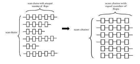
Scan chains
Each scan chain in DFT, acts as a single, long shift register for testing and the testing process involves shifting data in and out of these chains. If one chain is significantly longer than others, the test time is dominated by the longest chain, leading to inefficiencies

Negative edge triggered flip flops should be placed in the start of the chain.
If positive-edge flip-flops were placed first, the data might be captured on the rising edge of the clock and then “shot through” to the next positive-edge flip-flop before the negative-edge flip-flops could capture the data.
Fixing the flip flop order: In a scan chain, data is shifted through the flip-flops sequentially. When negative-edge flip-flops are placed first, they capture the input data on a falling edge, and positive-edge flip-flops capture the data on a rising edge. This arrangement helps to prevent data from being lost or misinterpreted during the shift operation.